 |
Miniaturization
Increased miniaturization will continue to yield ever high levels of efficiency. If the pace of technological innovation remains the same as it has been over the past decade, the density and speed of silicon chips will continue to double every 24 months (2 years). At that pace, transistor size will shrink approximately 30% per year. Over the same period of time, the cost per circuit will decline by 50%. The carrying capacity (i.e. bandwidth) of the cellular phone system will double every 9 months (.66 years). The capacity of optical memory devices (like CD-ROM’s) will double every 5 years. The carrying capacity of fiber optic cable will continue to double every 12 months (1 year).
|
 |
Chip Manufacturing Technology
- By the year 2020, the smallest feature on a microchip will be .01 micron wide. This is close to the physical limits of current (or foreseeable) technology. Unless micro device technology has a breakthrough, miniaturization is likely to stop. As the physical limits to miniaturization are approached, researchers will devise ways of growing larger and larger wafers so that chip harvests will continue to increase.
- Note the continuing development of X-ray lithography to fabricate microchips. Current production methods employ ultra-violet lithography to cut chip masks. Ultra-violet lithography however will soon reach limits imposed on the technology by the laws of physics. The need to produce smaller micro-components will fuel the development of a more advanced fabrication method (i.e. X-ray lithography).
|
 |
Chip Density
- By the year 2020, chip density will exceed 1 trillion components. A single, solid state memory chip will be capable of storing 64 billion bits of data.
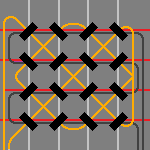
- By the year 2010, a single chip or wafer could contain 16 thousand 32 bit RISC processors, or 64 thousand 16 bit RISC processors or 1 million 1 bit RISC processors. By the year 2020, these figures could quadruple.
|
 |
High Density Magnetic Memory
Note the continued improvement in the density of magnetic media memory devices. This will result in hard disk capacity for a given disk size to increase substantially. Improved media density translates into reduced cost per unit of memory. As magnetic memory prices fall, note the introduction of mini-sized hard disks and removable media that are capable of economically holding prodigious amounts of data.
|
 |
High Density Solid State Memory Devices
Note the continued improvement in the density of solid state memory devices. The density of circuits on a solid state memory device will continue to double every two years for the foreseeable future. As density increases, solid state memory becomes an attractive alternative to other kinds of memory devices like removable hard disks or CD-ROM’s. Note the introduction of alternate types of solid state memory like flash memory.
|
 |
High Density Optical Memory Devices
Note the continued improvement in data storage equipment. Optical data storage methods continue to improve. By the year 2010, data density will be 4 times greater than the density available in the year 2000. For example, by the year 2010, 4.75” optical disks will contain 128 billion bits of data; 3” optical disks will contain 16 billion bits of data. At that density, the 3” optical disks could contain a feature length movie recorded in high definition TV. Smaller diameter optical disks will not be as cost effective or reliable as solid state memory devices. As a consequence, 2” optical disks will all but disappear.
|
 |
Optical Computers
- An optical computer uses laser light and glass fibers in place of copper wire and electrons to do its work. This highly experimental technology can, in theory, increase present day computational speeds a thousand fold. Such enormous increases in computational speed will radically alter how we use computers and what we use them for. At present, this technology is still immature. No practical applications have yet been demonstrated. As the technology develops (10 – 20 years), we can expect to see demonstrations in a wide variety of applications.
- The recent invention of optically based gates and switches bring the prospect of Optical Computing closer to reality. Optically based computer circuits would, in theory, operate faster and cooler than current technology. The technology remains highly experimental and years away from commercial introduction.
|
 |
Super Conductive Computer Circuits
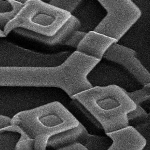
IBM recently announced the world’s first thin-film super conducting microcircuit that works at practical temperatures. This new device was manufactured through a process known as plasma spraying in which super conductive material is heated to its plasma state and sprayed onto the surface of a micro-chip. Advances such as this hold the promise of vastly more efficient computers in the not to distant future.
|
 |
Asynchronous Computer Chips
To date, virtually every computer ever made has been governed by the pulsing of its internal clock. Every aspect of a computer’s operations are timed to those pulses. Over time, designers have become quite skilled at creating chips with faster and faster clock speeds. Today for instance, computers are routinely clocked at 2.5 Gigahertz (i.e. 2.5 billion clock cycles). If history is any guide, clock speeds will continue to increase at a rate of 100% every 18 months.
As fast as these new computers are, they are still inherently inefficient. Tying computer operations to the ticking of a clock (no matter how fast that clock ticks) sometimes creates processing bottlenecks. Recently, a new type of “clock less” computer chip has been introduced onto the market. This new type of device allows electronic signals to pass through the chip without being stopped at timing gates. Without the timing gates, there is no need for an internal clock. Data is allowed to flow through the chip as fast as is physically possible. These new devices are called Asynchronous Computer Chips and they are fundamentally different from all previous CPU designs. Time will tell if these new chips prove to be more effective than traditional “synchronous” chips.
References:
Based on an article in Scientific American by Ivan E. Sutherland and Jo Ebergen entitled Computers Without Clocks (dated August, 2002).
|
 |
General Purpose, Reprogrammable Microchips (1 Chip Fits All)
Most microchips are designed for a specific function and contain special purpose microcircuits to optimize their performance. A new type of microchip has recently been invented that embodies an alternate design strategy. These new chips are general purpose devices that can be programmed to perform specific functions at will. They contain generic circuits that are capable of performing arithmetic and logical operations as well as store and retrieve data. These new chips are infinitely re-configurable. Circuit configuration is directly controlled through the use of an advanced software compiler. This is a fundamentally new way of organizing circuits on a chip.
Because these new chips mimic the performance of parallel computers, they hold the promise of revolutionizing the design and performance of small computers. Since these chips are inherently more efficient then current designs, their use is likely to further accelerate the diminishing cost of computing.
This new technology is still in its infancy and is highly experimental. Proof-of-concept chips have not yet been fabricated but prototype software compilers have been built and tested successfully. Despite the current state-of-the-art, researchers expect the technology to mature rapidly. They have predicted that by the year 2010, these chips will achieve clock speeds of 10 to 15 gigahertz.
|
 |
Wider Use of 64 bit CPU Chips
Intel has begun marketing a family of 64 bit CPU chips for use in the high end server market. This puts them in direct competition with well established companies like IBM, Motorola and Sun. Given Intel’s close alliance with Microsoft, we can expect any Intel marketing success to be accompanied by an increase in Microsoft‘s sales of it’s network operating system software. With such a direct threat looming and so much at stake, we can expect fierce competition to ensue. If Intel comes to dominate this new market like it does the PC market, product selection within the server market will be reduced. Thus, Intel and Microsoft’s entrance into this new market will probably trigger additional anti-trust scrutiny by federal and state governments.
|
 |
Magnetic Disk Drive Technology
- Hard disk capacity (measured in kilobits per square inch) grew about 25% – 30% per year in the 1980’s. In the 1990’s, hard disk capacity grew on average by 90% per year. By the end of 2001, hard disk capacity was growing at a rate of 130% a year. This year, hard disk capacity is doubling every 9 months.
- In 1988, the average cost for 1 megabyte of hard disk memory was $11.54. In 1998, the price for the same amount of memory had fallen to $0.04. In 2002, the price of hard disk space is $0.003 per megabyte.
- In September of 2000, hard disk density reached 10,000,000 kilobits per square inch. By March, 2002 hard disk density has reached 40,000,000 kilobits per square inch. By the end of 2002, hard disk density is expected to reach 80,000,000 kilobits per square inch.
- In May of 2000, hard disk capacity (using standard magnetic technology) averaged between 10 to 30 gigabits per square inch. Current predictions put the density limit of magnetic hard disk technology at about 150 gigabits per square inch. Hybrid storage devices are expected to reach a density of 200 gigabits per square inch.
- Disk storage will be used more efficiently in the future. Disk storage has gone from individual platters, to multiple platters (i.e. gangs of platters housed together), to disk arrays (i.e. gangs of ganged platters). In the not to distant future, we can expect wider use of storage area networks (i.e. pools of interconnected storage devices). We can also expect to see “storage farms” made up of unused disk space on PC workstations, enabled by advanced peer to peer networking techniques.
|
 |
Advanced Storage Technologies
- Magneto-Optical (Hybrid) storage devices have recently been introduced to the marketplace. Hybrid technology uses laser light to set the electromagnetic charge of the storage media. Disks produced in the year 2000 had a maximum capacity of 20 gigabytes.
- Improvements in storage media (i.e. the use of “Hard” Material technology) will enable hard disk densities to reach 1,000 gigabits (or 1 terabit) per square inch.
- The use of Patterned Magnetic Film technology will allow hard disk densities to reach 10,000 gigabits (or 10 terabits) per square inch.
- Holographic storage technology has been under development for (the past) 40 years. Working prototypes have recently been demonstrated but the technology is still years away from commercialization. When fully developed, holographic storage capacity could reach trillions of bytes per square inch.
- Additional improvements in storage media through the use of “Phase Change” technology will enable disk densities to reach 1,000 gigabits (or 1 terabit) per square inch. This technology is at least 10 years away from commercialization.
- IBM has recently demonstrated a microscopic punch card technology that is capable of storing 500 gigabits of data per square inch. The company plans to market improved versions of this device in the very near future. The mechanical limitations inherent with this technology limit the overall size of these devices. As a consequence, they will be marketed to manufacturers (like cell phone manufacturers and watch makers) who are designing very small devices but need prodigious amounts of memory and can’t use other storage technologies.
|
 |
Improved Storage Technology
- The cost of a storage bit is currently dropping at a rate of 1.5% per week.
- Experts agree that the current rate of density increase (130% per year) is not sustainable past 2005. There after, they expect to see the density growth rate fall to only 60% per year.
|
 |
CPU Road Map
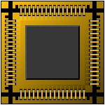
Looking ahead to 2010, chip manufacturers expect to see the performance of their microprocessors increase significantly. They also expect significant gains in their production efficiency. Actual chip performance estimates however, vary form manufacturer to manufacturer.
In 2001, Intel produced a microprocessor with a clock speed of 2.5 GHz. made from elements that were no larger then 0.18 microns. By the end of this year (2002), Intel expects to reduce the minimum element width to 0.15 microns. By the year 2003, chip speed will increase to 5 GHz and element width will shrink to 0.13 microns. In 2004, the element width is expected to shrink to 0.10 microns. By 2005, chip speed should increase to 10 GHz and element width will continue to shrink to 0.07 microns. At this density, Intel will be placing 400 million transistors on a single microprocessor chip. By the year 2005, the minimum element size will shrink to 0.05 microns.
By comparison, in the year 2000, American Micro Devices (AMD) produced a microprocessor with a clock speed of 1 GHz. made from elements that were no larger then 0.18 microns. By the end of this year, AMD plans to introduce a microprocessor with a clock speed of 2 GHz and a minimum element width of 0.13 microns. By the year 2006, AMD plans to package 2 microprocessors on the same chip. By 2010, AMD’s microprocessors will have a clock speed of 4 GHz. and a minimum element width of 0.07 microns. The wafer used to produce these chips will be 50 mm wide and each chip will contain 4 microprocessors.
In 2001, IBM introduced a line of microprocessors (i.e. the “Power4”) that had a minimum element width of 0.13 microns.
Applied Materials Corporation (AMC), a leading manufacturer of chip fabrication equipment, expects that by the year 2003, the minimum element size will drop to 0.10 microns. The silicon wafer used to produce these 0.10 micron chips will be 300 mm wide. By 2007, they expect chips to have a minimum element size of 0.045 microns. Chip speeds will increase to 20 GHz and chip densities will increase to 1 billion transistors. For comparative purposes, AMC’s current batch of chips has a minimum element width of 0.13 microns, a clock speed of 2 GHz and a density of only 42 million transistors.
References:
Applied Materials Corporation 2001 Annual Report.
|
 |
3D Chips
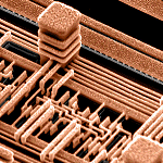
Fierce competition among chip manufacturers is driving researchers to find new ways to pack ever more transistors onto a single silicon wafer. Recently, engineers have begun to experiment with “layer cake” chip designs. This approach to miniaturization is very cost effective because it allows manufacturers to use familiar fabrication technology to significantly increase chip density. Since the cost of building an entirely new chip fabrication plant is enormous, we can expect manufacturers to exhaust the benefits of 3D chip making before making any such investment.
References:
Moore’s Law & Order by Rob Fixer; published in eWeek, April 15, 2002
|
 |
Carbon Nanotubes
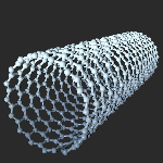
Engineers have begun experimenting with materials that might allow circuits to shrink beyond the limits imposed by the laws of physics on silicone based microchips. Recent attention has focused on specially configured carbon atoms called nanotubes. Nanotubes are made from rolled sheets of carbon that are only a few atoms thick. They are very dense, very strong and very cheap to manufacture. They also exhibit many of the same physical properties as silicone. Research is at an early stage. Do not expect to see commercial products based on this technology for at least five years.
References:
Moore’s Law & Order by Rob Fixer; published in eWeek, April 15, 2002
|
 |
Quantum Computing
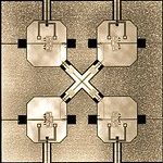
The current process of fabricating microchips may soon hit a physical limit. In an effort to circumvent these limits, scientists have begun experimenting with subatomic particles to discover if they can be used to carry information. This new approach has come to be known as Quantum Computing. It is highly theoretical and at least 10 to 15 years away from commercialization. Current research is focused on understanding how electrons behave in their quantum state.
References:
Moore’s Law & Order by Rob Fixer; published in eWeek, April 15, 2002
|